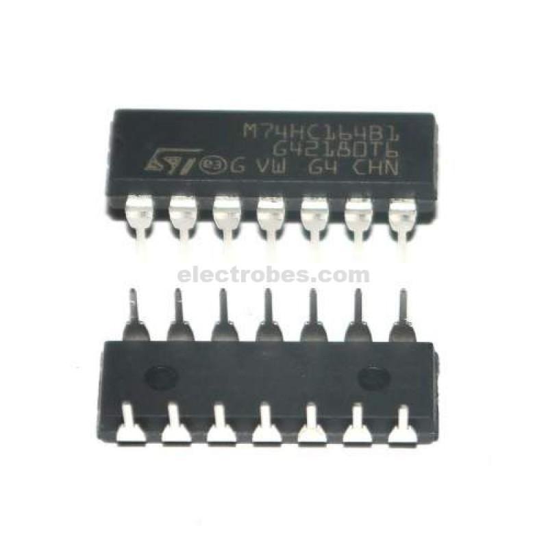
74HC164 8bit Serial-In / Parallel-Out Shift Register
- 8-bit Gated Serial Inputs with Asynchronous Clear
- Clocking Occurs on the Low-to-High Transition of the Clock Input
- Data at the Serial Inputs can be Changed on High or Low State of the Clock
- Standard TTL Switching Voltages
- Superseded, Not Recommended for New Designs
- Typical operating frequency: 50 MHz
- Typical propagation delay: 19 ns (clock to Q)
- Wide operating supply voltage range: 2V to 6V
- Low input current: 1 µA maximum
- Low quiescent supply current: 80 µA maximum
- Fanout of 10 LS-TTL loads
- Package type: DIP
- No. of pins: 14
In stock
₨ 30
In stock
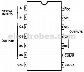
74HCT164 is an 8-bit serial-in/parallel-out shift register. The device features two serial data inputs (DSA and DSB), eight parallel data outputs (Q0 to Q7). Data is entered serially through DSA or DSB and either input can be used as an active HIGH enable for data entry through the other input. A LOW on the master reset input (MR) clears the register and forces all outputs LOW, independently of other inputs. Inputs include clamp diodes. This enables the use of current limiting resistors to interface inputs to voltages in excess of VCC. These 8-bit shift registers feature AND-gated serial inputs and an asynchronous clear (CLR) input. The gated serial (A and B) inputs permit complete control over incoming data; a low at either input inhibits entry of the new data and resets the first flip-flop to the low level at the next clock (CLK) pulse. Data is shifted on the LOW-to-HIGH transitions of the clock (CP) input. A high-level input enables the other input, which then determines the state of the first flip-flop. Data at the serial inputs can be changed while CLK is high or low, provided the minimum set-up time requirements are met. Clocking occurs on the low-to-high-level transition of CLK.
Features:
- Wide Operating Voltage Range of 2 V to 6 V
- Outputs Can Drive Up to 10 LSTTL Loads
- Low Power Consumption, 80-µA Maximum ICC
- Typical tpd = 20 ns
- ±4-mA Output Drive at 5 V
Based on 0 reviews
Be the first to review “74HC164 8bit Serial-In / Parallel-Out Shift Register”
You must be logged in to post a review.
Related products
-
Discrete Electronic Components, Resistors, Potentiometer & Knobs
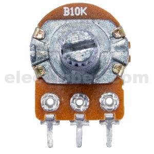
10K Ohm Rotary Potentiometer Variable Resistor Trimpot with Lever
 Discrete Electronic Components, Resistors, Potentiometer & Knobs
10K Ohm Rotary Potentiometer Variable Resistor Trimpot with Lever
This 10K trimmable potentiometer has a small knob built right in and it’s breadboard friendly to boot! Perfect for your next LCD contrast adjuster, opamp setting, or volume level. This model is B10K within the datasheet.
SKU: 0201

There are no reviews yet.