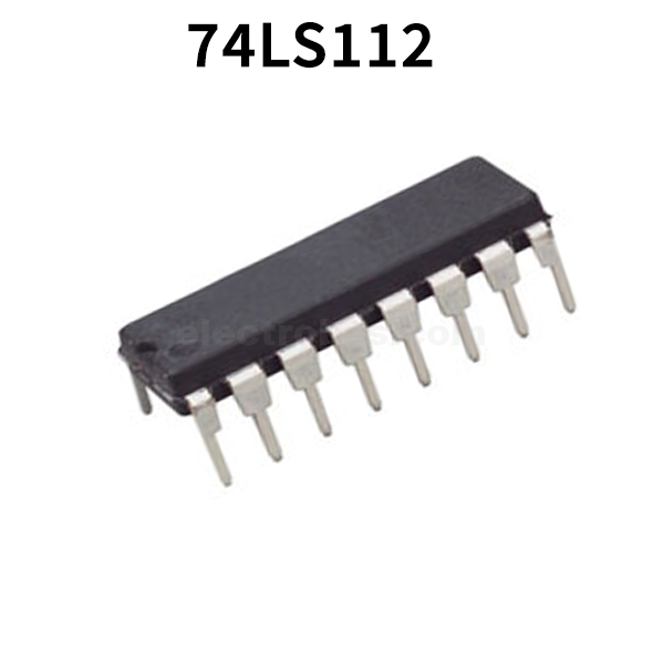
74LS112 Dual JK Negative Edge Triggered Flip-Flop IC
74LS76 comes with dual JK flip flops. JK flip flops are widely used in daily electronics devices by many methods but the basic operation of the JK flip flop is to store a bit. JK flip flop allows to store a bit and then allows it to use for further functions. in digital electronics circuits. JK flip flop is one of the popular flip flops due to its clock input, pre-set, and clear functionalities. The JK flip-flop changes its state under the clock pulse signal. The clock signal can be either a positive edge or a negative edge. The clock pulse gives multiple advantages to the flip flop. 74LS76 also has provided a feature to neglect or prevent invalid outputs.
Out of stock
₨ 120
Out of stock
74LS112 dual JK flip-flop features individual J, K, clock, and asynchronous set and clear inputs to each flip-flop. It contains two independent negative-edge-triggered J-K flip-flops with individual J-K, clock, and direct clear inputs. The 74LS112 IC has a wide range of working voltage, a wide range of working conditions, and directly interfaces with CMOS, NMOS, and TTL. The output of the IC always comes in TTL which makes it easy to work with other TTL devices and microcontrollers.
What is a JK Flip-Flop?
The JK Flip Flop is basically a gated RS flip flop with the addition of the clock input circuitry. When both the inputs S and R are equal to logic “1”, the invalid condition takes place. Thus to prevent this invalid condition, a clock circuit is introduced. The JK Flip Flop has four possible input combinations because of the addition of the clocked input. The four inputs are “logic 1”, ‘logic 0”. “No change’ and “Toggle”.
74LS112 Pinout:
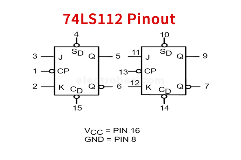
74LS112 Pin Configuration
| Pin No | Pin Name | Description |
|---|---|---|
| 1 | 1CLK | Clock Input 1 |
| 2 | 1K | Input Pin K1 |
| 3 | 1J | Input Pin J1 |
| 4 | 1PRE’ | Active low Preset Pin 1 |
| 5 | 1Q | Output pin Q1 |
| 6 | 1Q’ | Active Low output Pin Q1 |
| 7 | 2Q’ | Active Low output Pin Q2 |
| 8 | GND | Ground Pin |
| 9 | 2Q | Output pin Q2 |
| 10 | 2PRE’ | Active low Preset Pin 2 |
| 11 | 2J | Input Pin J2 |
| 12 | 2K | Input Pin K2 |
| 13 | 2CLK | Clock Input 2 |
| 14 | 2CLR’ | Active low clear/Reset pin 2 |
| 15 | 1CLR’ | Active low clear/Reset pin 1 |
| 16 | Vcc | Chip Supply Voltage |
74LS112 Features & Specifications
- Technology Family: LS
- Dual JK Flip Flop Package IC
- VCC (Min): 4.75V
- VCC (Max): 5.25
- No. of Bits: 2
- Operating Voltage (Nom): 5V
- Frequency at normal voltage (Max): 35MHz
- Propagation delay (Max): 20ns
- IOL (Max): 8mA
- IOH (Max):-0.4mA
Applications
- PCs and notebooks
- Digital Electronics
- Shift Registers
You can download this Datasheet for 74LS112 Dual JK Negative Edge Triggered Flip-Flop from here
- Technology Family: LS
- Dual JK Flip Flop Package IC
- VCC (Min): 4.75V
- VCC (Max): 5.25
- No. of Bits: 2
- Operating Voltage (Nom): 5V
- Frequency at normal voltage (Max): 35MHz
- Propagation delay (Max): 20ns
- IOL (Max): 8mA
- IOH (Max):-0.4mA
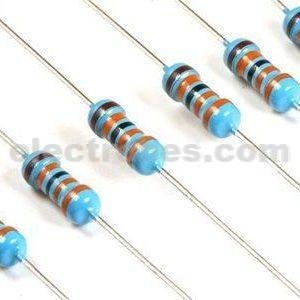
Related products
-
Discrete Electronic Components, Resistors, Potentiometer & Knobs
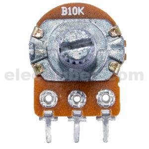
10K Ohm Rotary Potentiometer Variable Resistor Trimpot with Lever
 Discrete Electronic Components, Resistors, Potentiometer & Knobs
10K Ohm Rotary Potentiometer Variable Resistor Trimpot with Lever
This 10K trimmable potentiometer has a small knob built right in and it’s breadboard friendly to boot! Perfect for your next LCD contrast adjuster, opamp setting, or volume level. This model is B10K within the datasheet.
SKU: 0201