Analog, Discrete Electronic Components, ICs
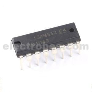
CD4049 Hex Inverter Buffer IC
CD4049 is a general purpose Hex Inverter Buffer IC. CD4049 holds six inverter gates on a single package. The IC works on the voltage range from 3V to 15V excessive voltage more than 15V will destroy the IC. So provide input voltage in the range of 3V to 15V. The IC invert the binary input i-e if we apply 1 at input it will out 0 and vice versa
Availability:
Out of stock
₨ 30
Out of stock
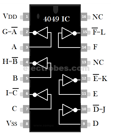
Pin Configuration
| Pin Number | Pin Name | I/O | Description |
| 1 | VDD | – | Positive supply for IC |
| 2 | G | O | Inverting output 1 for input 1 |
| 3 | A | I | Input 1 |
| 4 | H | O | Inverting output 2 for input 2 |
| 5 | B | I | Input 2 |
| 6 | I | O | Inverting output 3 for input 3 |
| 7 | C | I | Input 3 |
| 8 | VSS | – | Negative supply for IC |
| 9 | D | I | Input 4 |
| 10 | J | O | Inverting output 4 for input 4 |
| 11 | E | I | Input 5 |
| 12 | K | O | Inverting output 5 for input 5 |
| 13 | NC | – | Not connected |
| 14 | F | I | Input 6 |
| 15 | L | O | Inverting output 6 for input 6 |
| 16 | NC | – | Not connected |
Features
- Mostly used in voltage multiplier circuit
- Accept High input supply voltage
- Used to low the high logic levels
- High sink current for driving two TTL loads
- Special input protection allows input voltages greater than VDD
- 100% Tested for Quiescent Current at 20 V
- Available packages: PDIP, SOIC, TSSOP, SO with 16 number of pins
- Maximum input current of 1uA at 18v over full package temperature range
- Compatible in use with breadboard.
Datasheet :
http://www.ti.com/lit/ds/symlink/cd4050b.pdf
- Input supply voltage ranges from 3v (min.) to 18v (max.)
- Supply current 50mA (max.)
- Ambient Temperature ranges from -40 to +85°C
- Input capacitance is 22.5pf (max.)
- As input voltage increase from 5v to 15v, output current sink also vary from 1.8 to 26mA
Based on 0 reviews
Be the first to review “CD4049 Hex Inverter Buffer IC”
You must be logged in to post a review.

There are no reviews yet.